News
HOME
News
All
News
Exhibition Information
Technical Articles
Media Coverage
VIEW 162
2025.11.23
Exhibition Information
Meet Top Seiko at Semicon Japan 2025
VIEW 180
2025.08.06
Technical Articles
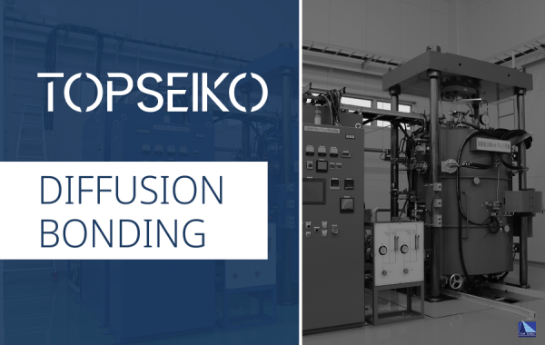
What Can Diffusion-Bonded Components Really Do?
VIEW 153
2025.06.06
Technical Articles
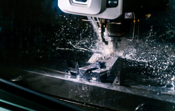
Why Precision Machining Costs More – and Why It’s Worth It