We introduce machining examples of silicon
Silicon, being the same material as wafers, is used to prevent contamination and particles in semiconductor manufacturing
Polycrystalline (columnar) materials are available in large sizes. Polycrystalline materials offer better machinability with less chipping and cracking than single crystal
Silicon(Si)
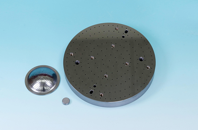
No Contamination (Same as Wafer Material) · Resistivity Control
Compatible with Diffusion BondingTypical properties of silicon
| Item | Vickers Hardness HV (GPa) |
Flexural Strength (MPa) | Melting Point (℃) |
Coefficient of Thermal Expansion (×10-⁶/℃) |
Thermal Conductivity (W/(m·K)) |
Volume Resistivity (μΩ・㎝) |
Purity (%) |
Doping Type |
|---|---|---|---|---|---|---|---|---|
| Crystal Structure / Chemical Formula | ||||||||
| Single Crystal (Si) |
7 | 78 | 1,414 | 3.4 | 160 | 0.1–100 | 11N | N P |
| Polycrystalline (Si) |
7 | 85 | 1,414 | 3.3 | 163 | 0.001–10 | 6N | P |
Machinable Sizes
| Item | Sizes (mm) | Item | Sizes (mm) |
|---|---|---|---|
| Plate Dimensions | 500 × 800 ×50 (Polycrystalline) | Hole Diameter | Φ0.03– |
| Rod Dimensions | Φ100 ×400 (Polycrystalline) | Hole Depth | 20D(–Φ1.5)、400(Φ1.5–) |
| Grooves | Width 0.05– | Number of Holes | –5,000 |
| Steps (Protrusions / Recesses) | –100 | Threads | M3~ (Requires insertion of a helical insert) |