Core Technologies
Precision Machining and Diffusion Bonding of Advanced Materials
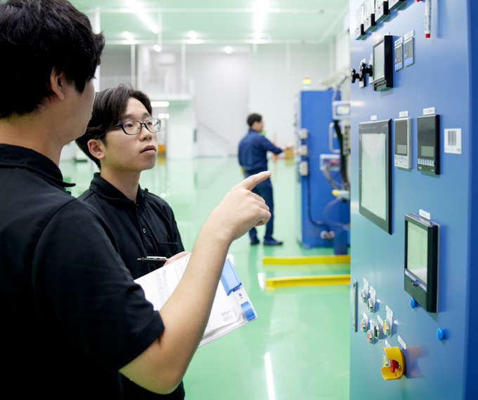
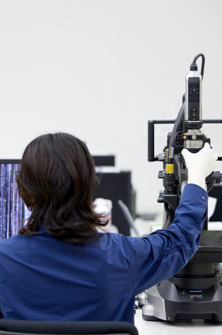
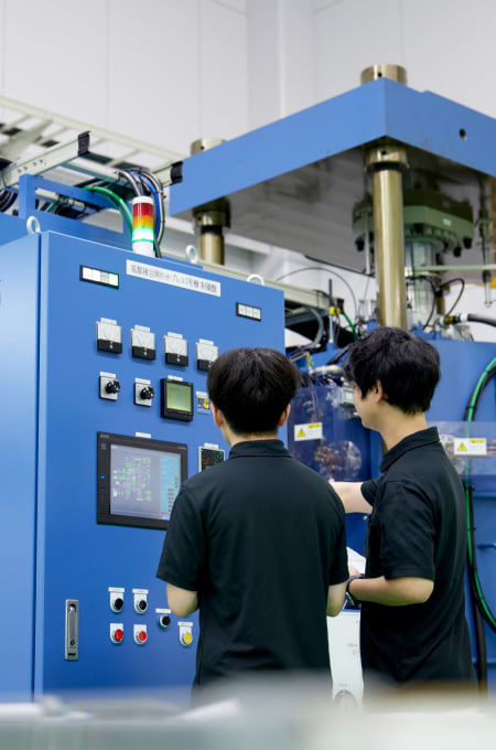
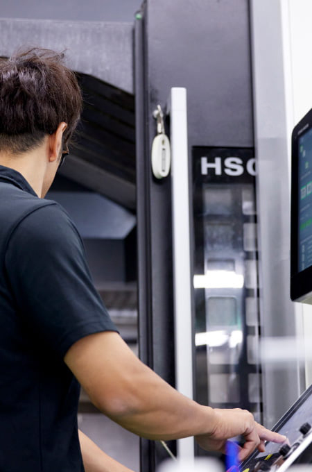
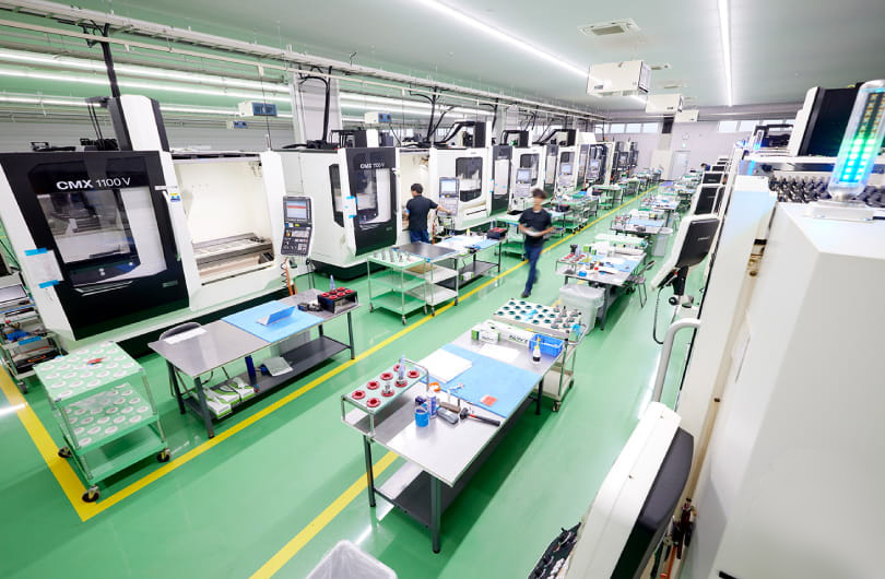
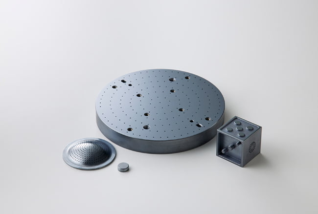
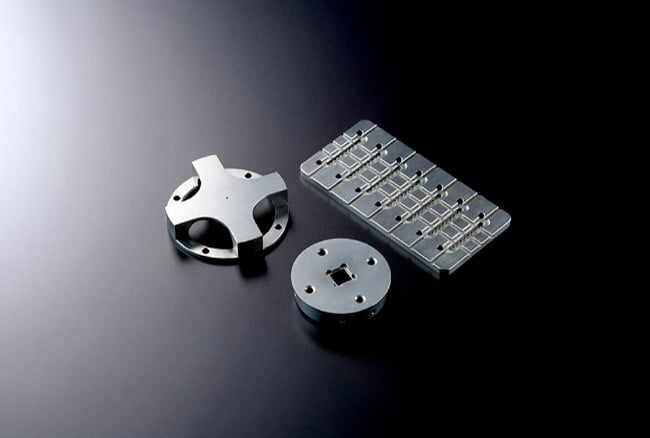
Since its founding, Top Seiko has supplied critical components requiring extremely tight tolerances to equipment manufacturers across a wide range of industries, including semiconductor, aerospace, electronics, and automotive. Our core technologies are precision machining of advanced materials and diffusion bonding. We have extensive experience in machining advanced ceramics as well as refractory metals such as molybdenum and tungsten.
Precision Machining
of Advanced Materials
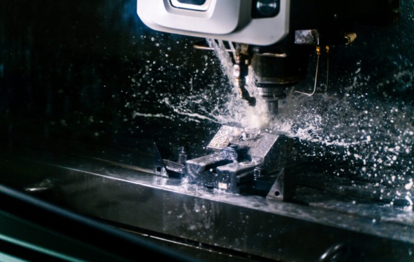
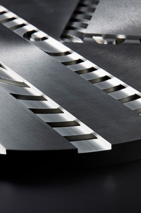
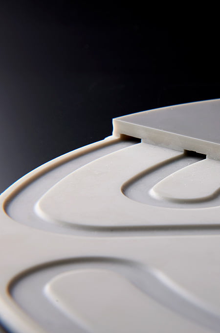
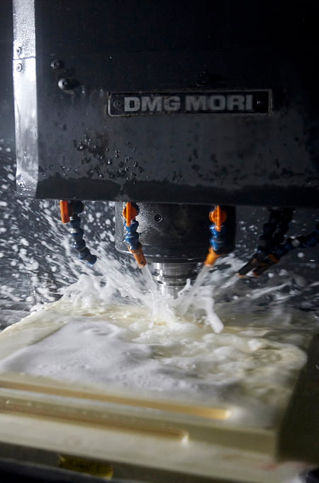
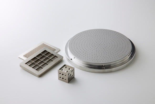
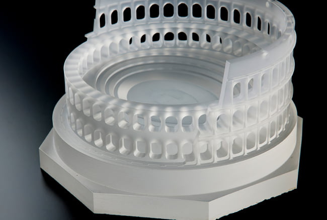
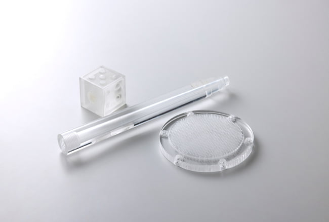
We possess a broad range of specialized technologies that enable us to machine advanced materials—including ceramics, refractory metals, and quartz glass—into complex, high-precision geometries exactly as required.
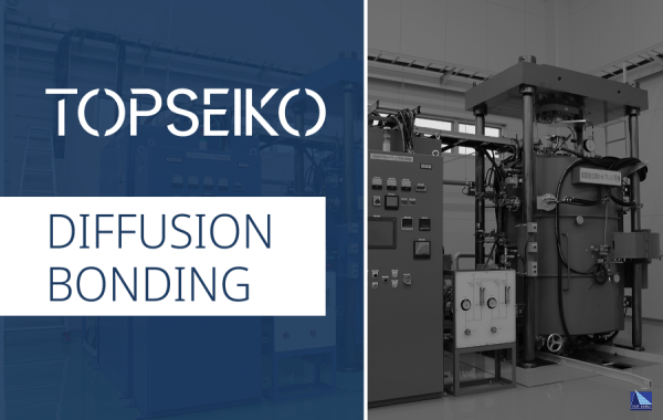
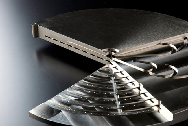
Diffusion Bonding
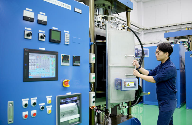
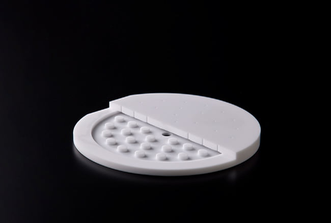
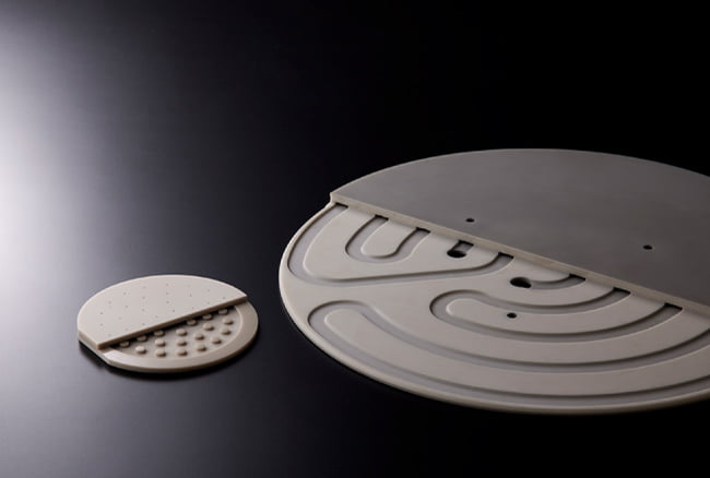
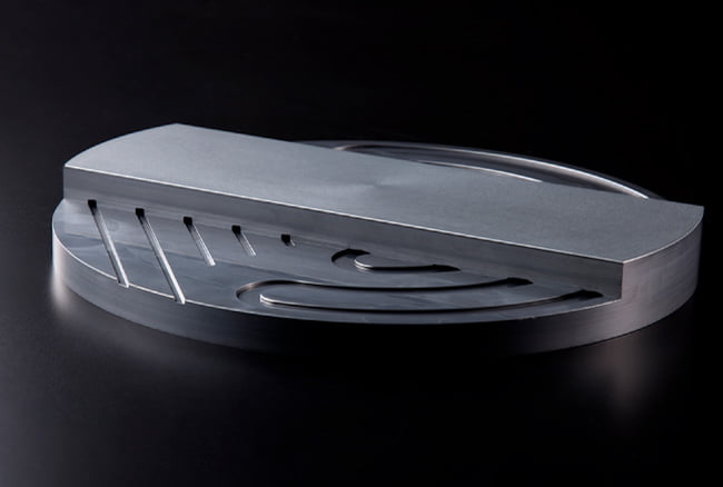
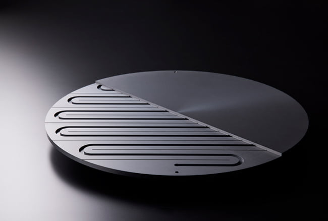
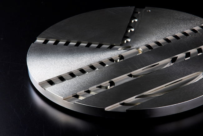
Through advanced diffusion bonding technology, materials are joined in the solid state—without melting—by atomic-level diffusion. This enables the creation of highly reliable, high-performance components and supports innovation across advanced industries.
Applications by Material
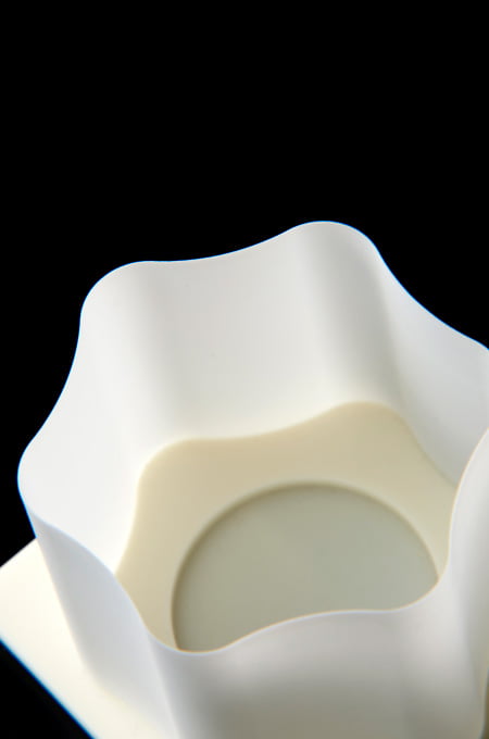
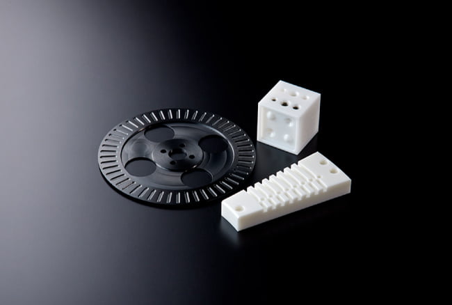
We present machining examples of sample components manufactured by Top Seiko, organized by material. We invite you to explore these examples as a reference for your applications.
Ceramics
-
Alumina (Al₂O₃)
Electrical Insulation · High Strength · Heat Resistance · Wear Resistance · Plasma Resistance · Chemical Resistanc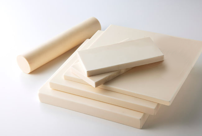 Compatible with Diffusion Bonding
-
Aluminum Nitride (AlN)
High Thermal Conductivity · Heat Resistance · Electrical Insulation · Low Thermal Expansion · Plasma Resistance · Chemical Resistance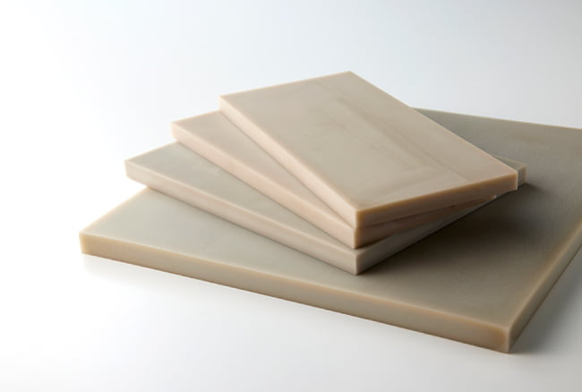 Compatible with Diffusion Bonding
-
Zirconia (ZrO2)
High Fracture Toughness · Wear Resistance · Low Thermal Conductivity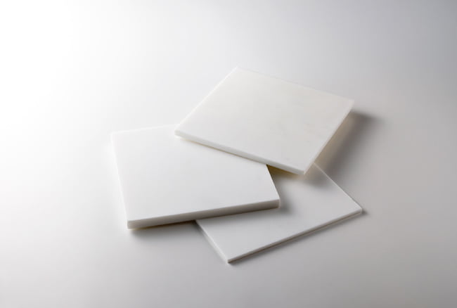
-
Silicon Carbide (SiC)
High Hardness · High Stiffness · High Thermal Conductivity · Corrosion Resistance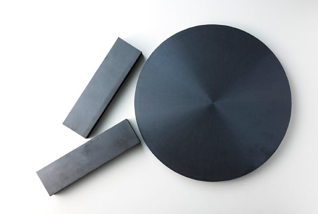 Compatible with Diffusion Bonding
-
SiSiC (Silicon-Infiltrated Silicon Carbide)
High Stiffness · Low Thermal Expansion · Heat Resistance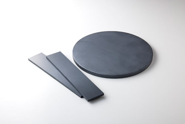 Compatible with Diffusion Bonding
-
Silicon (Si)
Contamination-Free (Wafer-Equivalent Material) · Controlled Resistivity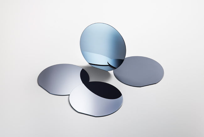 Compatible with Diffusion Bonding
-
Machinable Ceramics
Electrical Insulation · Heat Resistance · Excellent Machinability
Refractory Metals
-
Molybdenum (Mo)
High-Temperature Resistance · High Thermal Conductivity · Low Thermal Expansion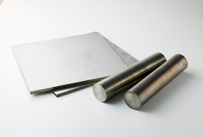 Compatible with Diffusion Bonding
-
Tungsten (W)
High-Temperature Resistance · High Thermal Conductivity · Low Thermal Expansion · High Density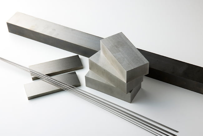
-
Tantalum (Ta)
Electric Insulation・High-Temperature Resistance · Good Machinability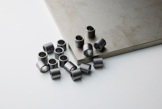
-
Niobium (Nb)
High-Temperature Resistance · Superconducting Properties · Corrosion Resistance · Biocompatibility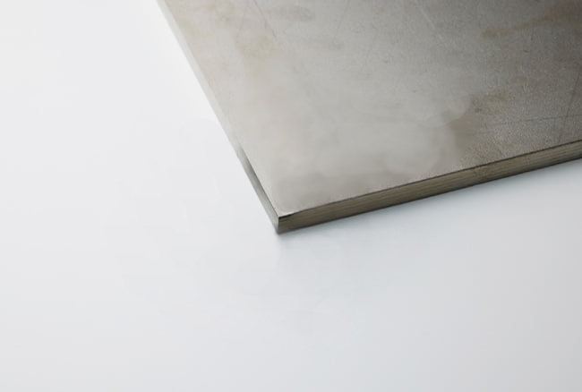
Advanced Metals
-
Nickel (Ni)
Corrosion Resistance · High-Temperature Resistance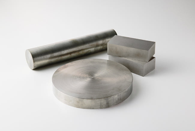 Compatible with Diffusion Bonding
-
Titanium (Ti)
High Strength · Lightweight · Good Machinability · Corrosion Resistance · Biocompatibility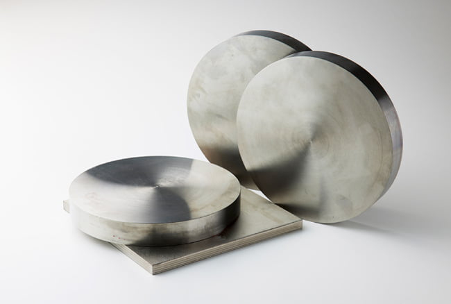
Glass
-
Quartz Glass / Heat-Resistant Glass
High-Temperature Resistance · Low Thermal Expansion · Electrical Insulation · Chemical Resistance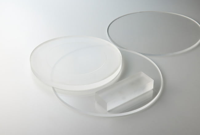 Compatible with Diffusion Bonding
-
Sapphire (Al₂O₃)
Optical Transparency · High Hardness · High Strength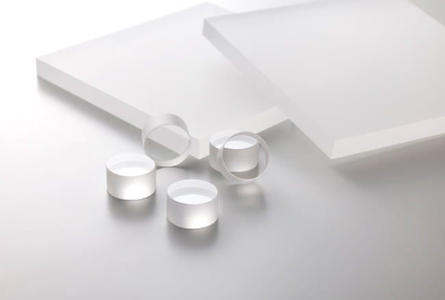
Material Guide
Explore by Properties
Search by Specifications
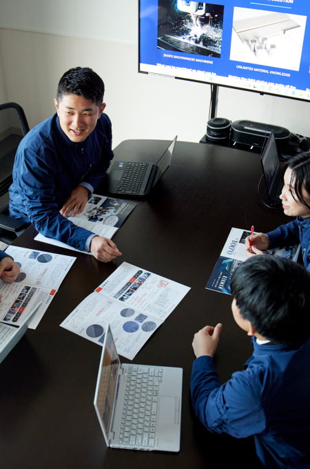
Development Support
Contributing to our customers’ new product development
through two core technologies
Precision machining of difficult-to-machine materials and diffusion bonding.
By leveraging these two core technologies to supply custom mechanical components, we create new value for industries around the world.
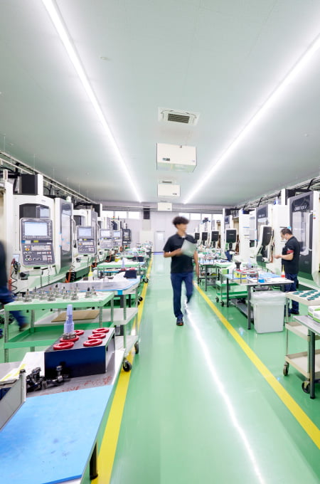
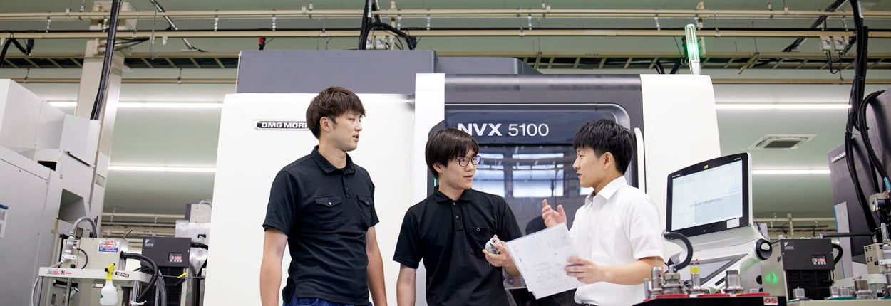
Our extensive inventory of materials, a wide range of machining equipment, and the technical expertise built on the experience of skilled engineers enable us to support the rapid launch of our customers’ new product development.