
Exploring the Complex World of Semiconductor Etching Processes
2024.07.05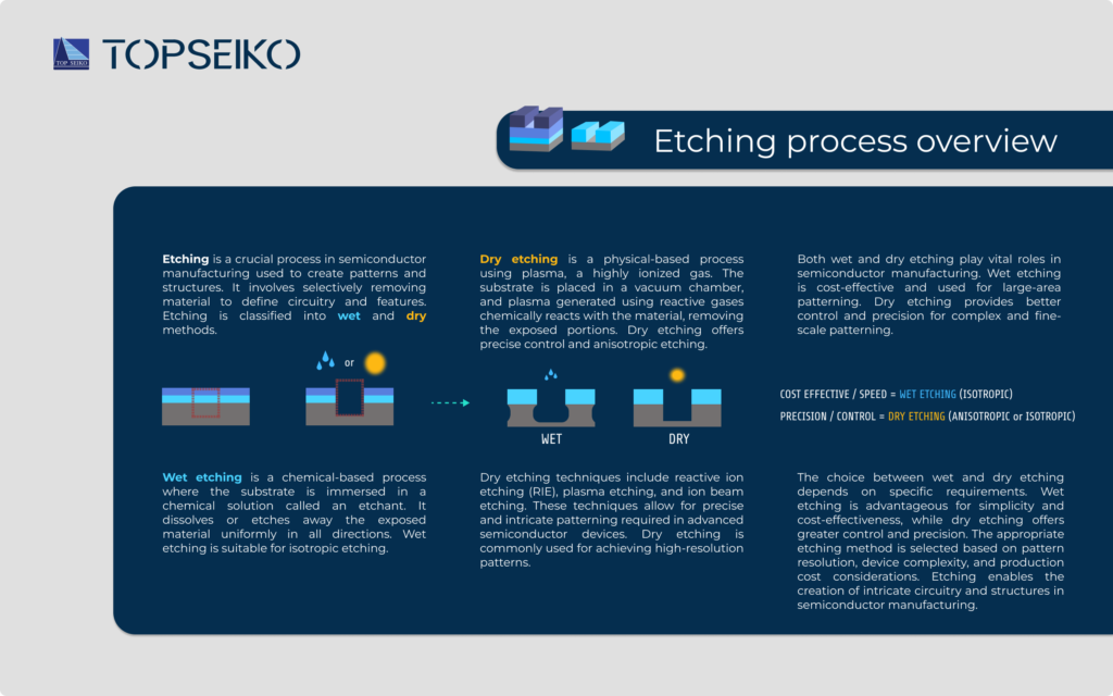
Etching is a critical process in semiconductor manufacturing that is used to create intricate patterns and structures.
It involves selectively removing material to define circuitry and features.
Etching methods are broadly categorized into wet and dry techniques.
Wet etching utilizes chemical solutions, known as etchants, where the substrate is immersed.
The etchant dissolves or etches away the exposed material uniformly in all directions. This method is suitable for isotropic etching.
On the other hand, dry etching relies on physical processes using plasma—a highly ionized gas.
The substrate is placed in a vacuum chamber, where plasma generated from reactive gases reacts chemically with the material, removing the exposed portions.
Dry etching allows for precise control and offers anisotropic etching capabilities.
Dry etching techniques encompass reactive ion etching (RIE), plasma etching, and ion beam etching, all enabling the intricate patterning essential for advanced semiconductor devices. It is particularly favored for achieving high-resolution patterns.
Both wet and dry etching methods are indispensable in semiconductor manufacturing.
Wet etching is cost-effective and ideal for large-area patterning, while dry etching provides superior control and precision, crucial for complex and fine-scale patterns.
The choice between wet and dry etching hinges on specific manufacturing requirements.
Wet etching offers simplicity and cost-effectiveness, whereas dry etching ensures greater precision and control.
The optimal method is selected based on factors such as pattern resolution, device complexity, and production costs.
Precision manufacturing plays a pivotal role in choosing between these methods. For example, Top Seiko manufactures custom wafer carriers and handling tools used in transporting and positioning semiconductor wafers during the etching process. These carriers are typically crafted from advanced materials like ceramics or glasses to ensure precise alignment, protection, and contamination control of the wafers.
We collaborate closely with semiconductor equipment manufacturers to develop and fabricate these advanced parts.
Our materials and manufacturing processes are tailored to meet the stringent requirements of the semiconductor industry, including high precision, tight tolerances, and compatibility with semiconductor processes.
For further information or technical support, please do not hesitate to contact us !
For Our LiknedIn profile > LINKEDIN
Together, let’s shape the future of semiconductor technology with precision and innovation !
