Enhancing Semiconductor Production with Vacuum Chucks
2024.10.01
The semiconductor industry has experienced significant breakthroughs in chip performance, largely driven by advancements in circuit miniaturization and multi-layering techniques. Among these developments, 3D packaging and hybrid bonding are two standout technologies in mid-end semiconductor manufacturing.
At Top Seiko, we specialize in delivering premium vacuum chucks crafted from a variety of materials, designed to meet the demands of these advanced manufacturing processes. Our vacuum chucks are tailored to meet the specific requirements of each customer, ensuring precise and reliable performance.
For applications requiring rapid heat transfer, a rigid structure, or a close match to the thermal expansion coefficient of silicon wafers, we recommend vacuum chucks made from Silicon Carbide (SiC) or SiC-based composite materials (MMC).
These materials offer superior thermal conductivity and strength, making them ideal for high-performance operations.
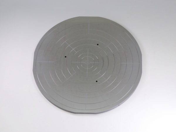
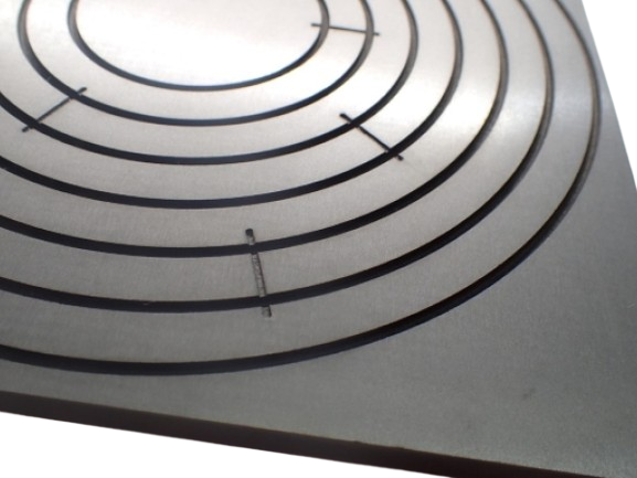
 Product name: φ180, 2mm concentric groove
Material used: SS701
Processing details: A groove with a width of 2mm was cut with an outer diameter of approximately 180.
Notes: The depth is 2.0mm. It has a high thermal conductivity.
Alternatively, when heat insulation, minimal thermal expansion, or optical transparency for substrate inspection are critical, quartz glass is the ideal material. It provides excellent insulation properties and allows for visual inspection through the substrate, making it a versatile option.
In addition to material selection, the flatness of the vacuum chuck’s top surface is critical for proper wafer handling.
At Top Seiko, we utilize NAGASE’s ultra-precision grinding technology to achieve an industry-leading flatness of 0.003 mm, and in some cases, we can meet even more demanding specifications.
We also offer a range of customization services, including heli-coil insertion, coating, and polishing, to ensure our vacuum chucks meet your exact needs.
Contact us today to learn how we can support you in reaching your technological goals.
Further Reading and Resources:
For more detailed information on high-performance materials and their applications, visit the Top Seiko News Blog.
At Top Seiko, we are dedicated to delivering high-precision solutions that meet the growing challenges of semiconductor manufacturing !


