Semiconductor Oxidation Process Overview – Top Seiko
2023.06.01🔎 Semiconductor Oxidation Process Overview 🔎
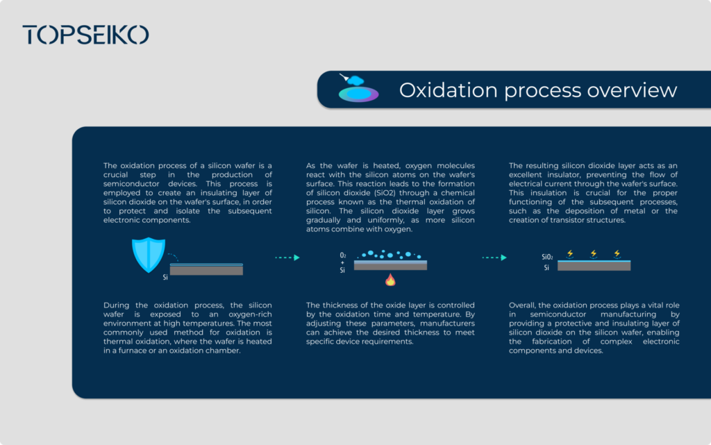
The oxidation process of a silicon wafer is a crucial step in the production of semiconductor devices. This process is employed to create an insulating layer of silicon dioxide on the wafer’s surface, in order to protect and isolate the subsequent electronic components.
During the oxidation process, the silicon wafer is exposed to an oxygen-rich environment at high temperatures. The most commonly used method for oxidation is thermal oxidation, where the wafer is heated in a furnace or an oxidation chamber.
As the wafer is heated, oxygen molecules react with the silicon atoms on the wafer’s surface. This reaction leads to the formation of silicon dioxide (SiO2) through a chemical process known as the thermal oxidation of silicon. The silicon dioxide layer grows gradually and uniformly, as more silicon atoms combine with oxygen.
The thickness of the oxide layer is controlled by the oxidation time and temperature. By adjusting these parameters, manufacturers can achieve the desired thickness to meet specific device requirements.
The resulting silicon dioxide layer acts as an excellent insulator, preventing the flow of electrical current through the wafer’s surface. This insulation is crucial for the proper functioning of the subsequent processes, such as the deposition of metal or the creation of transistor structures.
Overall, the oxidation process plays a vital role in semiconductor manufacturing by providing a protective and insulating layer of silicon dioxide on the silicon wafer, enabling the fabrication of complex electronic components and devices.
Top Seiko can create custom-made substrate holders or wafer carriers used to position and hold the semiconductor wafers during the oxidation process. These holders can be made from materials like quartz or ceramic, providing stability and thermal resistance.
Creating precision parts using advanced materials ensures stability, accuracy, contamination control, thermal management, chemical compatibility, process optimization, and customization. These factors collectively contribute to the overall efficiency, reliability, and success of semiconductor manufacturing processes.
Follow Top Seiko on LinkedIn for the latest updates and industry insights. 🗞️
Or contact us directly to learn more about our services in depth!


