Semiconductor Lithography Process Overview – Top Seiko
2023.08.09Semiconductor Lithography Process Overview
Semiconductor lithography is a crucial process in the manufacturing of semiconductor devices, such as microchips and integrated circuits. It involves the precise transfer of intricate patterns onto a silicon wafer, which serves as the foundation for these electronic components.
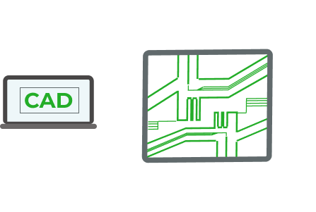
The process begins with the creation of a photomask or reticle, which is a glass plate containing a pattern of the desired circuitry. This mask design is typically generated using computer-aided design (CAD) software.
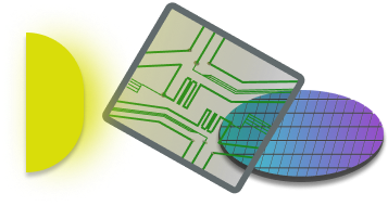
The photomask is carefully aligned with the coated wafer, and the combination is exposed to ultraviolet (UV) light or an electron beam. The light or beam passes through the transparent regions of the mask and interacts with the photoresist on the wafer, initiating a chemical reaction.
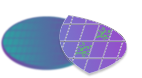
The exposure causes the photoresist to undergo a physical or chemical change, making it either more soluble or less soluble in a subsequent developing process. The areas exposed to light become either more soluble (positive photoresist) or less soluble (negative photoresist), depending on the type of resist used.
Advanced lithography techniques, such as optical lithography, extreme ultraviolet (EUV) lithography, or electron beam lithography, are employed to achieve higher resolutions and smaller feature sizes, enabling the production of more intricate and powerful microchips.
As you know advanced materials play important roles in various components and equipment used in photolithography.
Top Seiko can manufacture custom-made holders for photomasks , stage components and much more.
Holders, typically made from materials like ceramics or metals, provide stability and precision alignment for the photomask during exposure to ensure accurate pattern transfer onto the semiconductor wafer.
To encapsulate the intricate process of semiconductor manufacturing, the stages are designed to provide high precision, stability, and repeatable motion. They often incorporate advanced materials, such as ceramics, metals, or specialized coatings, to ensure thermal stability, rigidity, and compatibility with the process environment. The precise control of stages is essential for achieving tight tolerances, high yield, and consistent device performance in semiconductor fabrication.
Follow Top Seiko on LinkedIn for the latest updates and industry insights. 🗞️
Or contact us directly to learn more about our services in depth!